Thin Film Technology

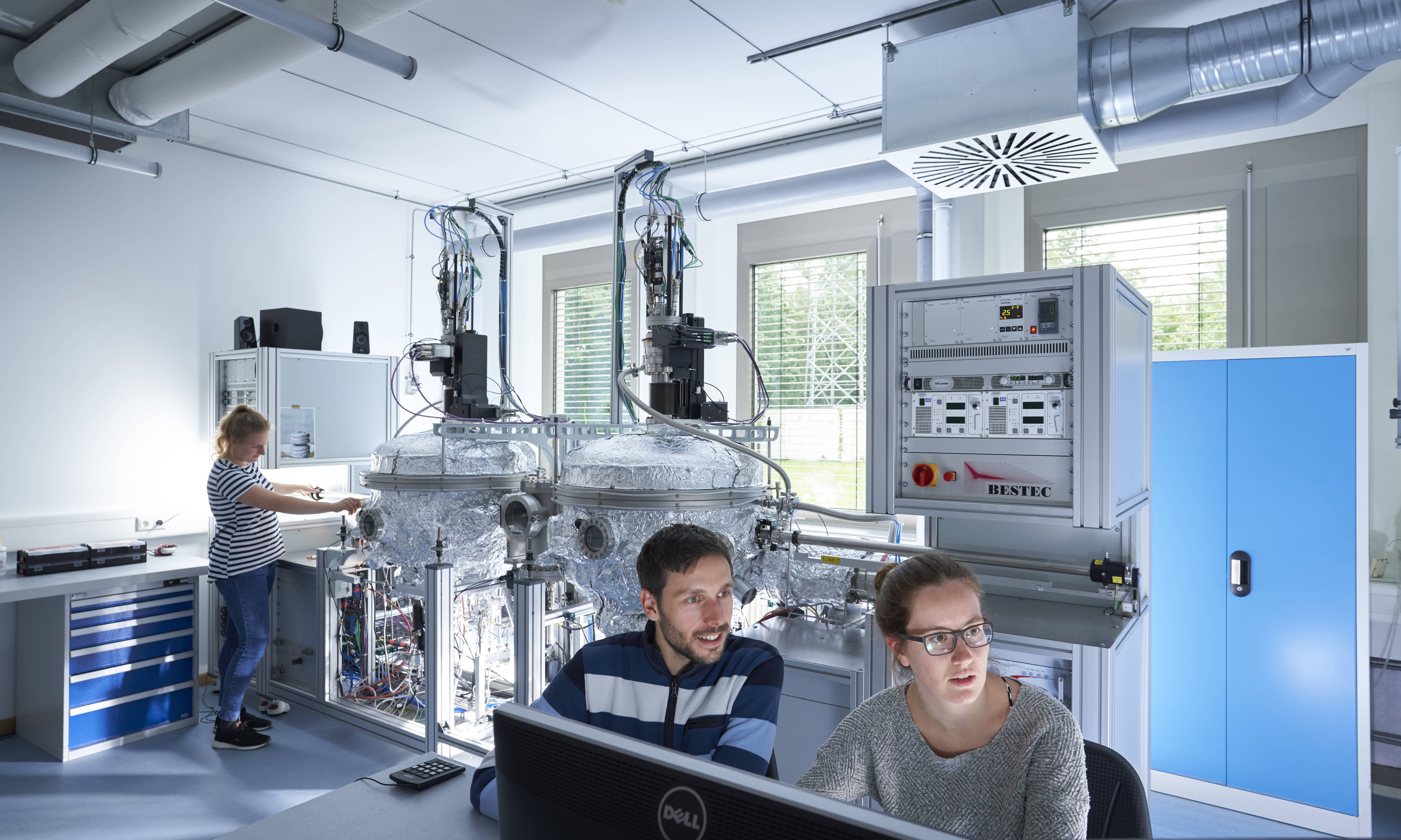
The WMI operates a flexible UHV Laser-Molecular Beam Epitaxy (L-MBE) system, designed to meet the special requirements of oxide hetero-epitaxy. It is used for the heteroepitaxial growth of complex oxide multilayers consisting of superconducting, dielectric, (anti)ferromagnetic, ferroelectric, and semiconducting materials. The L-MBE systems is combined with an electron beam deposition and a sputtering system in a UHV cluster tool. In this way it allows for the combination of oxide heterostructures with metallic (superconducting, magnetic) thin films without breaking vacuum.
For the fabrication of superconducting quantum bits and quantum circuits, WMI operates a PLASSYS MEB 550 S4-I UHV system. It allows for the fully automated deposition of superconducting thin films required for the fabrication of Al- and Nb-based superconducting quantum circuits. It consists of a loadlock and two further UHV chambers for sputter deposition of niobium and titanium and for electron beam deposition of aluminium and titanium. The systems is equipped with a flexible sample holder for shadow evaporation and an oxidation chamber, allowing for the controlled fabrication of oxide tunnel barriers required for Josephson junctions.
The WMI also operates two UHV sputter deposition systems, which allow for the fully-automated fabrication of complex metallic multilayers of superconducting and magnetic materials. The first UHV system is dedicated to the deposition of high-quality superconducting thin film and heterostructures (e.g. Al, Nb, NbN, NbTi, NbTiN) required for superconducting resonators, trasnmission lines, or superconducting single photon detectors. The second UHV system consists of two separate UHV chambers connected via the joint load-lock chamber. One chamber is dedicated to superconducting materials (e.g. Nb, NbN, Ta, TaN) and the other to magnetic materials (e.g. Fe, Co, Py, CoFe) and nonmagnetic metals (Pt, Ir). By the two-chamber solution, cross-contamination between superconducting and magnetic materials is avoided. However, superconducting and magnetic thin flims can be also combined in e.g. superconductor/ferromagnet heterostructures, as the samples can be transferred between the two chambers under vacuum conditions.
