Materials, Methods and Infrastructure
WMI has a comprehensive research effort on materials and operates a large variety of experimental methods for materials and device characterization. With respect to material synthesis, our activities are focused on thin film technology and single crystal growth. For device fabrication, we operate extensive technological infrastructure, allowing for the generation of device structures down to the 10 nm regime.
Our research program is focused on the
- synthesis of superconducting and magnetic materials,
- single crystal growth of oxide materials,
- thin film technology of complex superconducting and magnetic heterostructures, including multi-functional and multi-ferroic material systems,
- fabrication of solid-state based quantum systems, such as superconducting quantum bits and circuits, and the
- fabrication of superconducting, magnetic, mechanical, and hybrid nanostructures.
For the implementation of our research program we operate various state-of-the-art equipment for thin thin film deposition, single crystal growth, and micro- and nanopatterning. This includes, for example, several UHV deposition systems as well as a clean room with a 100 kV electron beam lithography system, an optical laser beam writer, a mask aligner, and a RIE system.
The WMI operates a flexible UHV Laser-Molecular Beam Epitaxy (L-MBE) system, designed to meet the special requirements of oxide hetero-epitaxy. It is used for the heteroepitaxial growth of complex oxide multilayers consisting of superconducting, dielectric, (anti)ferromagnetic, ferroelectric, and semiconducting materials. The L-MBE systems is combined with an electron beam deposition and a sputtering system in a UHV cluster tool. In this way it allows for the combination of oxide heterostructures with metallic (superconducting, magnetic) thin films without breaking vacuum.
For the fabrication of superconducting quantum bits and quantum circuits, WMI operates a PLASSYS MEB 550 S4-I UHV system. It allows for the fully automated deposition of superconducting thin films required for the fabrication of Al- and Nb-based superconducting quantum circuits. It consists of a loadlock and two further UHV chambers for sputter deposition of niobium and titanium and for electron beam deposition of aluminium and titanium. The systems is equipped with a flexible sample holder for shadow evaporation and an oxidation chamber, allowing for the controlled fabrication of oxide tunnel barriers required for Josephson junctions.
The WMI also operates two UHV sputter deposition systems, which allow for the fully-automated fabrication of complex metallic multilayers of superconducting and magnetic materials. The first UHV system is dedicated to the deposition of high-quality superconducting thin film and heterostructures (e.g. Al, Nb, NbN, NbTi, NbTiN) required for superconducting resonators, trasnmission lines, or superconducting single photon detectors. The second UHV system consists of two separate UHV chambers connected via the joint load-lock chamber. One chamber is dedicated to superconducting materials (e.g. Nb, NbN, Ta, TaN) and the other to magnetic materials (e.g. Fe, Co, Py, CoFe) and nonmagnetic metals (Pt, Ir). By the two-chamber solution, cross-contamination between superconducting and magnetic materials is avoided. However, superconducting and magnetic thin flims can be also combined in e.g. superconductor/ferromagnet heterostructures, as the samples can be transferred between the two chambers under vacuum conditions.
The clean room is equipped with the standard tools for photolithography such as resist coaters, hot plates, wet benches, a Karl Süss MJB3 mask aligner, and the direct laser writing system PicoMaster 200. It further hosts a reactive ion etching system with ICP plasma source.
Finally, the 100 kV e-beam lithography system nB5 is installed in the second part of the clean room facility. The nB5 is a round-beam step-and-repeat system oriented towards high-end R&D applications at universities and research institutes for nanopatterning and mixed-match lithography.
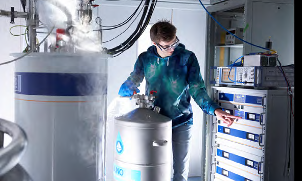
The WMI operates numerous dry dilution fridges...
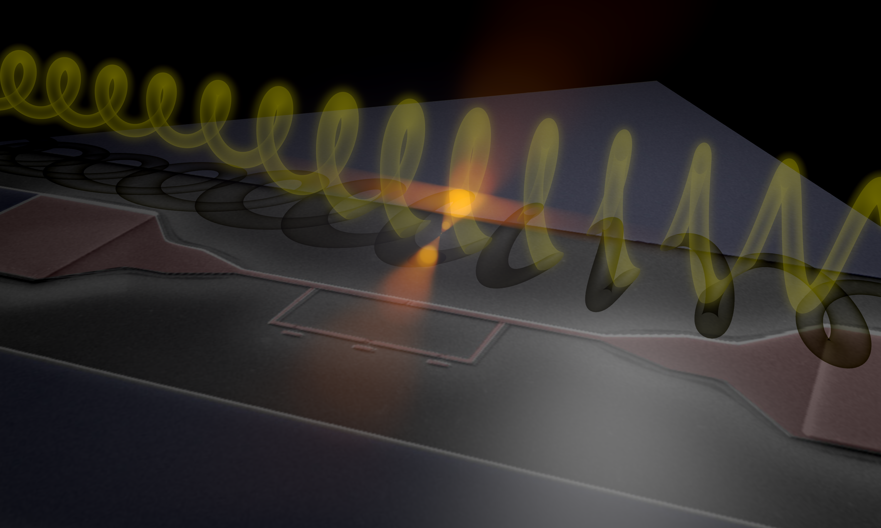
The Walther-Meissner-Institute pioneered superconducting quantum circuits representing quantum optical experiments. This research requires the generation of microwaves with tailored properties and the development of detection techniques which allow to extract quantum signature of the signal. Researchers at the WMI developed the hardware and the analysis strategies and successfully demonstrated them in several seminal experiments.
The techniques developed here, are not exclusively used for experiments involving superconducting circuits, but also find applications for the more general set of experiments involving microwaves in quantum science experiments, including quantum sensing and quantum materials.
Three of them (14 T, 16 T, and 15/17 T) are located in the high-field laboratory in the upper floor of the WMI.
Another 3D vector magnet with variable temperature insert, allowing for 2.5 T in-plane and 6 T out-of-plane magnetic fields, is available for thermal and electrical transport experiments since 2018. It contains a vertically oriented 6 T solenoid combined with two horizontally oriented split-coil pairs.
A further 3D vector magnet allowing for 1 T in-plane and 6 T out-of-plane magnetic fields is installed in the WMI Quantum Laboratories as part of a cryogen-free dilution system.
At the Walther-Meissner-Institute we use this technique to investigate the magnetic properties of bulk materials, thin film systems and multilayer systems. This allows us to quantify static magnetic properties like the saturation magnetization, magnetic anisotropies and the type of the magnetic order. In addition, this technique allows to study the dynamical properties of magnetic excitations like magnetic damping.
We are also developing and using techniques with are employ the excitation of the magnetic system using magnetic resonance techniques and complement those with electronic or optical readout concepts. This allows to address questions regarding the excitation and detection of spin currents and the spatially propagation on spin excitations.
Besides various chamber- and tube furnaces a four-mirror image furnace is used for the crystal growth of various oxide systems. Many different compounds of the high temperature superconductors and various other transition metal oxides have been grown as single crystals using the traveling solvent floating zone technique. The furnace consists basically of 4 elliptical mirrors with a common focus on the sample rod and with halogen lamps in their other focus. Single
crystal growth can be performed with this furnace at maximum temperatures up to 2200 C in the pressure range from 10-5 mbar up to 10 bar and in oxidizing, reducing as well as inert atmosphere.